 Rongqiangbin

Global Commercial Landscape of Semiconductor Wafer Testing
The semiconductor industry's rapid evolution, driven by artificial intelligence (AI), 5G telecommunications, high-performance computing (HPC), and automotive electronics, has positioned wafer testing as an indispensable phase in the silicon manufacturing value chain. Wafer testing—historically categorized under Wafer Sort (WS) or Circuit Probe (CP)—is the process of electro-mechanically verifying the viability of individual dies while still on the silicon wafer. It acts as the gatekeeper of microelectronic yield management.
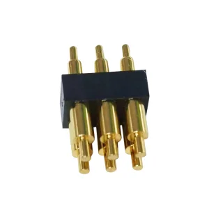
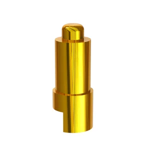
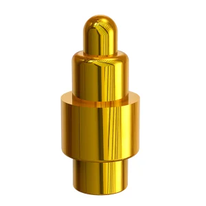
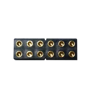
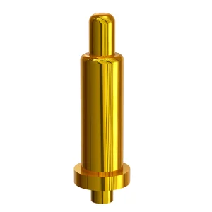
As microchip architectures shrink to sub-3nm nodes and integrate complex 2.5D/3D Advanced Packaging technologies (like CoWoS and WLCSP), the cost of packaging a defective die has become prohibitively high. Consequently, wafer testing manufacturers and suppliers face intense pressure to deliver contact pins and sockets that maintain low, stable contact resistance over millions of cycles, at extremely tight pitches (often down to 0.2mm or less).
"The primary objective of modern wafer testing component supply chains is minimizing the Cost of Test (CoT) without compromising test signal fidelity, positioning cost-optimized precision manufacturing at the center of semiconductor growth."