Explore our top-tier precision spring-loaded sockets and probe pin solutions engineered for modern electronics testing.
In the highly complex world of semiconductor manufacturing, the Wafer Probe Testing Process stands as one of the most critical stages. It represents the first physical test performed on individual integrated circuits (ICs) while they are still clustered on the silicon wafer. The primary objective is to weed out defective dies prior to the expensive packaging phase, ensuring that only "Known Good Die" (KGD) advance down the line. To achieve this, automated test equipment (ATE) drives micro-fine spring probe pins (often engineered in customized test sockets) to establish direct electrical contact with microscopic bond pads, solder bumps, or micro-pillars on the wafer.
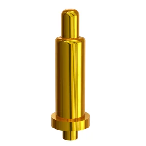
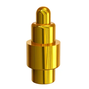
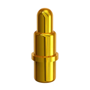
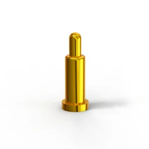
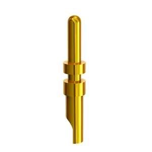
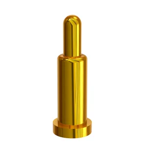
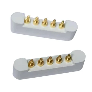
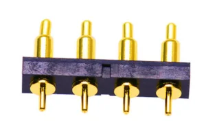
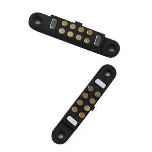
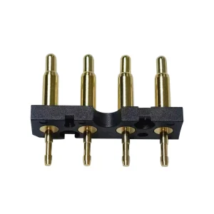
At Shenzhen Rongqiangbin Electronic Hardware Co., Ltd., we design, engineer, and manufacture the fundamental hardware driving this process. High-performance pogo pins and custom probe sockets act as the electrical highway between the wafer under test and the parametric analytical systems. As wafers shrink and density increases, the mechanical demands on these contact pins become tighter. Engineers require zero signal attenuation, stable contact resistance, and extreme life cycles—traits that only an ODM expert can guarantee.
Analyzing individual dies on the wafer substrate for capacitance, resistance, threshold voltage, and leak currents to isolate substrate defects early.
By mapping out failing chips digitally before slicing and dicing, OEMs save millions in packaging resources, elevating the overall production yield.
Providing custom pins configured for pitch dimensions under 0.5mm, maintaining absolute geometric precision without contact deviation.
Leading GBA Connector Technology Development Since 2011
Our company was founded in February 2011 in Songgang Street, Shenzhen, specializing in the development and manufacturing of Pogopin connectors. After years of focused engineering and strategic technological sedimentation, the company gradually rose to become a recognized leader in the high-precision connector industry.
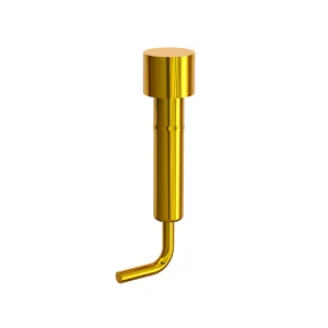
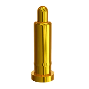
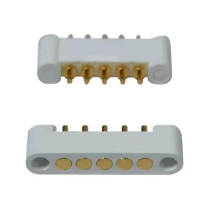
We are primarily engaged in the research, development, production, and sales of various models of POGO PIN (also known as spring thimbles) and complex socket assemblies. Governed by the core spirit of "customer first, integrity first," our strong production technology and design engineering teams form the bedrock of our high-reliability solutions.
We have successfully established long-term cooperative partnerships with an array of world-renowned enterprises, including Honeywell, Samsung, SIEMENS AG, ZTE, 360, QCY, HAYLOU, Shanghai Laimu, Luxshare Group, Aoni Electronics, and Amphenol Group.
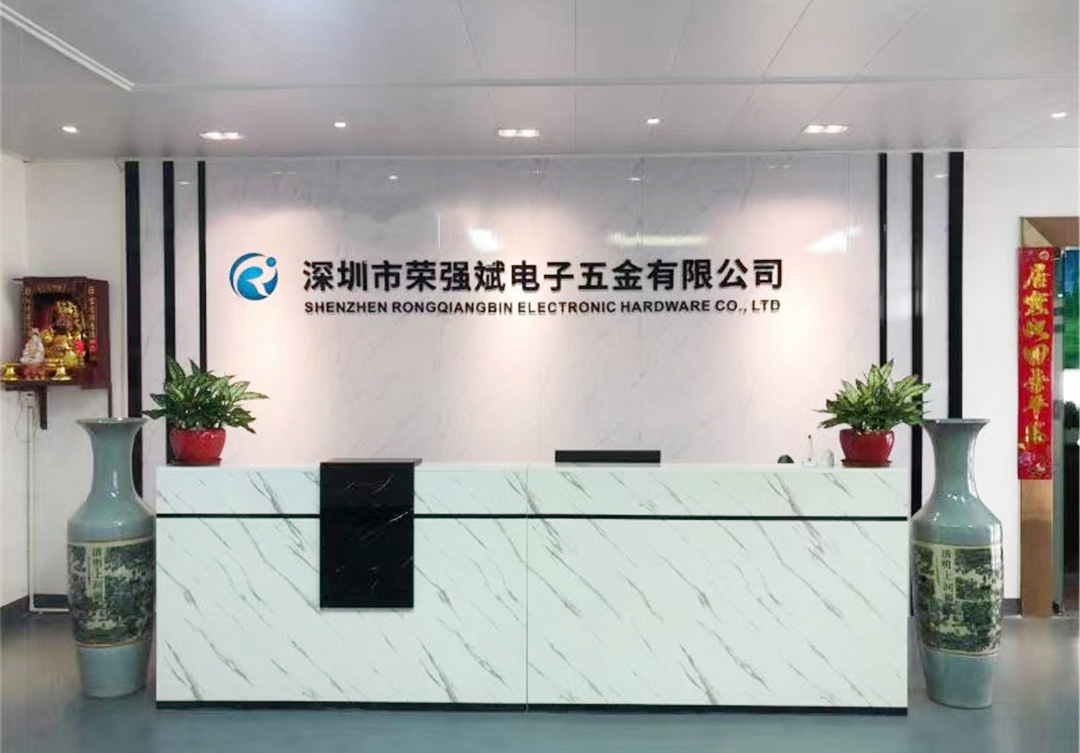
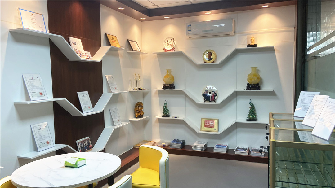
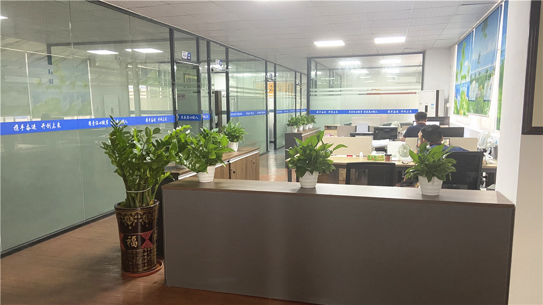
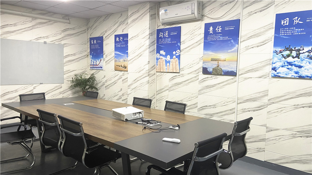

"Committed to being an excellent POGO PIN manufacturer for both quality and cost at home and abroad, and leading connector technology development into the future."
For procurement and test engineers, specifying the right contact elements is the difference between project success and costly downtime.
Wafer probing operates at high frequencies, demanding low self-inductance and low contact resistance (usually < 50 mOhms). Our proprietary plunger designs maximize internal surface contact, minimizing signal degradation during RF and high-speed digital tests.
Too much force can crack or damage the delicate wafer pad structure. Too little force fails to pierce the oxide layer, leading to false failures. Rongqiangbin designs precision springs that provide stable forces (e.g., 15-30g) within a defined working travel range.
Testing must often occur at extreme temperatures (-40°C to +150°C) to simulate real-world operations. We utilize specialized base metals and custom gold-plating matrices to prevent thermal deformation and spring fatigue under extended temperature cycling.
With thick, high-durability gold plating, our contact pins resist wear, corrosion, and solder contamination, ensuring consistent performance over millions of touchdown cycles.
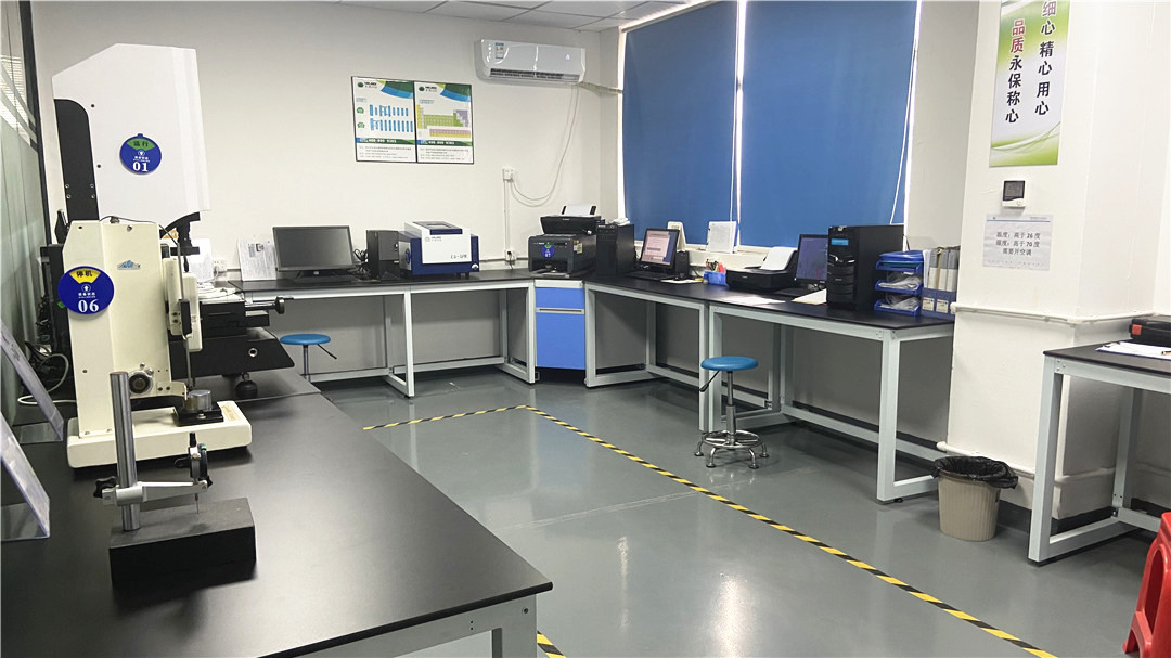
We operate state-of-the-art manufacturing facilities. With our in-house lathe turning, precise automatic assembly, and meticulous quality inspection systems, we deliver absolute dimensional stability for every batch.
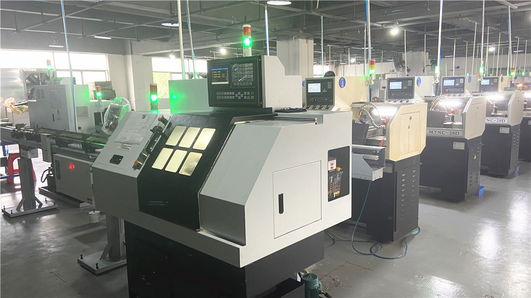
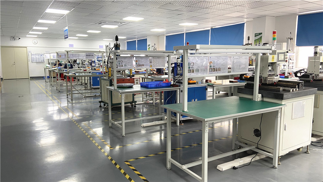
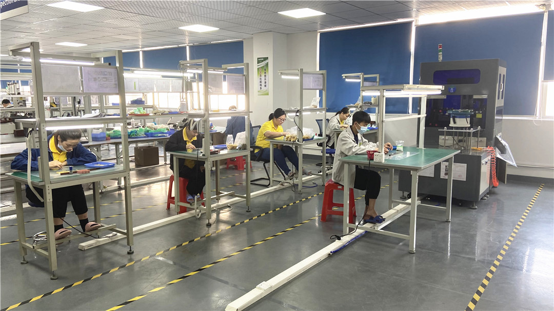
How Rongqiangbin bridges the gap between high-volume manufacturing and strict international standards.
Our high-precision spring contact structures are deployed across critical technology sectors globally.
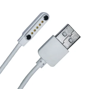
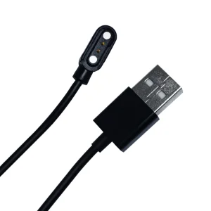
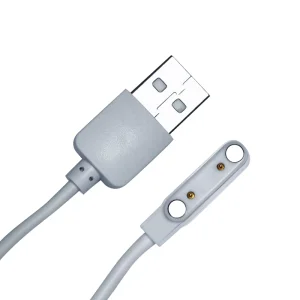
Wristbands, smartwatches, and Bluetooth headsets (QCY, HAYLOU). Our custom gold-plated pogo pins provide high corrosion resistance against sweat and moisture.
Laptops, mobile antennas, digital cameras, and learning machines. High-speed signal stability ensures zero loss during high-volume production testing.
Military communications, GPS satellite navigation, and aerospace electronics. High-reliability spring mechanisms resist shock, vibration, and temperature extremes.
Critical medical devices and smart industrial automation systems (Honeywell, Siemens). Clean materials and precision contact geometry offer stable current paths.
As the semiconductor industry progresses toward 3nm, 2nm, and even smaller silicon processes, the demand on the wafer probe testing ecosystem is undergoing a dramatic shift. Here are the key developments reshaping the industry:
Answers to common industry queries regarding wafer testing processes, spring probe selection, and supplier collaboration.
The spring-loaded probe acts as the temporary, highly stable electrical interface between the individual die pads on a silicon wafer and the external Automated Test Equipment (ATE). Its spring function ensures constant contact force, compensating for height variations on the wafer surface, while its high-conductivity plating guarantees clean signal flow.
We operate under a strict ISO9001:2015 Quality Management System. Tolerances on our precision lathe turnings are controlled to within microns (±0.005mm). We also utilize advanced automated optical inspection (AOI), X-ray thickness measurement devices for plating layers, and dynamic force/stroke curve testers to guarantee unit consistency.
Typically, we use Beryllium Copper (BeCu) or Paliney 7 for the plunger tips, which are hardened and plated with high-purity gold (Au) or Rhodium-Ruthenium over nickel. This combination maximizes electrical conductivity while resisting the abrasive wear caused by contact with aluminium oxide or tin-lead residue.
Yes. As an ODM supplier, we collaborate directly with your testing and hardware packaging teams. You provide us with the chip package dimensions or pad map, and our R&D team will design the complete test socket assembly, housing materials (PEEK, Torlon, or POM), and internal pin geometries to match your test fixture.
Depending on the design, stroke displacement, and environment, our high-durability test pins achieve lifecycles between 100,000 and 1,000,000 cycles. We recommend regular cleanings using ultrasonic systems or specialized cleaning sheets to remove surface contaminants and maintain optimal performance.
High-reliability connector systems designed for consumer tech, telecom, and industrial testing environments.
 Rongqiangbin