Explore our industrial-grade contact assemblies designed for reliability, electrical fidelity, and extended testing lifecycle.
In the ultra-competitive global semiconductor supply chain, manufacturing efficiency is determined by yield optimization. The primary line of defense in protecting integrated circuit (IC) yield is Wafer-Level Testing. Before individual silicon dies are cut from a processed wafer and sent to final packaging, they undergo rigorous Automated Test Equipment (ATE) checks. This stage ensures that only "Known Good Dies" (KGD) progress forward, preventing the costly mistake of packaging defective silicon.
At the physical boundary of this critical test cycle lies the Wafer Test Probe. Acting as the electromechanical bridge between the micro-scale pads of the wafer and the macro-scale diagnostic circuitry of the ATE system, these contact pins must maintain continuous electrical continuity under demanding mechanical conditions. As global logic designs push boundaries into sub-3nm nodes, and memory architectures stack into 3D configurations (like high-bandwidth memory or HBM3e), the demand for high-reliability, custom-engineered ODM Wafer Test Probes has grown exponentially.
Early identification of micro-defects at the wafer level significantly reduces downstream packaging losses, saving up to 40% of total manufacturing costs in multi-chip module (MCM) packages.
Engineered to operate at high frequencies (up to 40 GHz and beyond) with minimal insertion loss and controlled characteristic impedance matching.
Specifically developed to survive millions of contact actuations (touchdowns) against rugged materials like Aluminum pads or Lead-Free Solder micro-bumps.
A wafer probe is not just a structural element; it is an active mechanical assembly subjected to extreme cyclic stresses. As an industry-leading ODM Wafer Test Probe Manufacturer, Shenzhen Rongqiangbin Electronic Hardware Co., Ltd. applies structural mechanics and advanced materials science to create high-performance probe systems. The components must balance mechanical toughness with electrical conductivity.
Standard semiconductor test probes face localized resistance heating, surface oxidation, and wear-induced tip deformation. Our engineering team utilizes premium alloys to overcome these challenges:

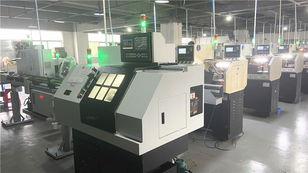
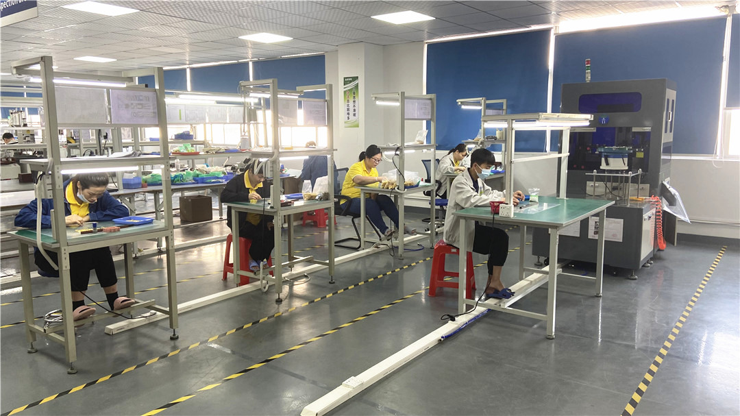
Figure 1: Shenzhen Rongqiangbin manufacturing infrastructure utilizing advanced micro-machining lathes.
To prevent localized galvanic corrosion and material migration at high temperatures, our contact probes undergo advanced electroplating processes. Heavy gold plating (Au) over a barrier layer of nickel (Ni) ensures stable electrical resistance. For high-frequency ATE applications, we optimize the skin depth by plating layers of precious metals, reducing surface roughness and maintaining signal integrity in RF testing.
Insertion Lifespan
Typical Contact Resistance
Year of Establishment
Certified Quality System
Specializing in the development and manufacturing of premium Pogo Pin connectors and spring-loaded testing components since February 2011.
Founded in Songgang Street, Shenzhen, within the highly active Guangdong-Hong Kong-Macao Greater Bay Area, our company has built a reputation for engineering high-precision contact products. Our commitment is simple: to be an excellent POGO PIN and test contact manufacturer for both quality and cost, leading the development of connector technology.


While precision testing components are designed to perform on micro-scale wafer pads, the downstream applications of these validated chips span almost every segment of modern technology. Our wafer test probes and customized spring contacts enable quality validation across these key areas:
Ensures the flawless validation of high-density SoC chips deployed in smart wearable products (wristbands, watches), laptops, and Bluetooth headsets (e.g., QCY, HAYLOU). Reliability is verified at wafer scale to avoid system failures in miniaturized consumer electronic products.
Wafer-level validation of sensor chips, GPS satellite navigation components, and aerospace micro-electronics. Test probes must withstand wide temperature profiles during thermal characterization tests (-40°C to 125°C).
High-reliability wafer test setups validation for leading telecommunication chipsets (ZTE), smart home hubs (360), medical equipment controllers, and industrial processing systems engineered by Honeywell and Siemens.

We maintain long-term cooperative relationships with Honeywell, Samsung, SIEMENS AG, ZTE, 360, QCY, HAYLOU, Shanghai Laimu, Luxshare Group, Aoni Electronics, Amphenol Group, and other well-known global enterprises.
As packaging architectures shrink, grid pitches reduce from 150 microns down to 80 microns and below. This requires the development of Micro-Spring Probes. Traditional cantilever designs are giving way to Vertical Probe Cards using arrays of miniature spring contact pins (Pogopins).
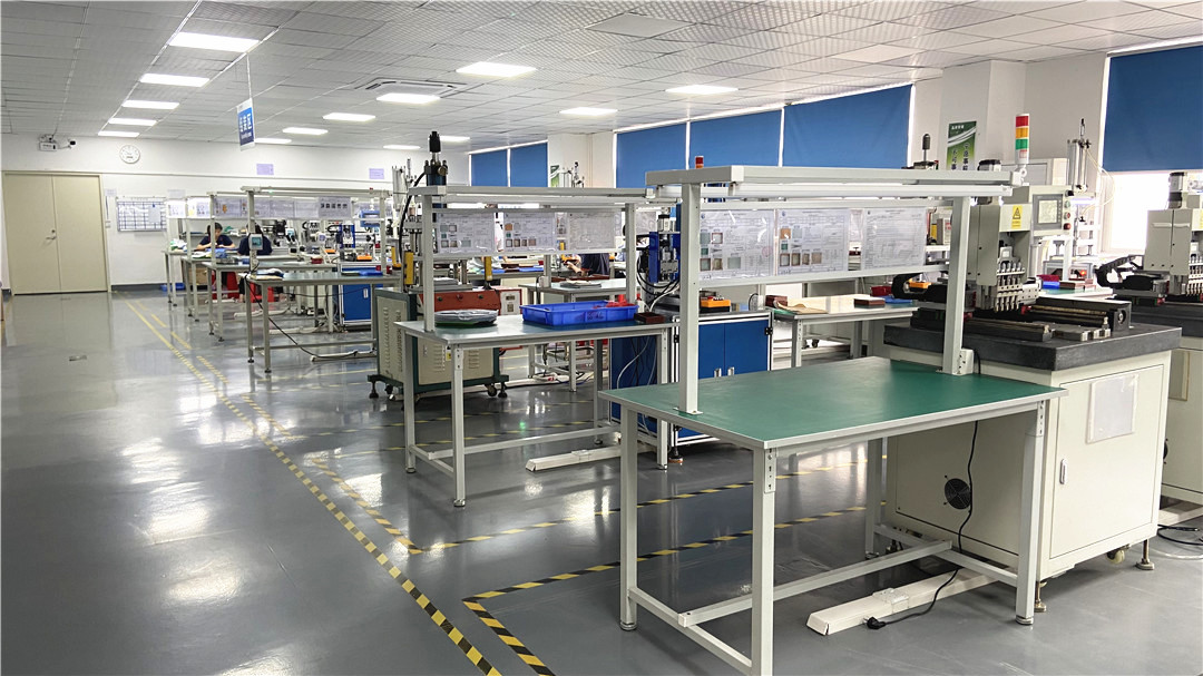
Shenzhen Rongqiangbin Electronic Hardware Co., Ltd. addresses this transition directly. Our production facility leverages state-of-the-art precision CNC lathes and automated inspection equipment to achieve tight manufacturing tolerances, ensuring precise positioning accuracy and uniform spring pressure.
Operating under the ISO9001:2015 quality management system to deliver high reliability and environmental compliance.
We prioritize a "Customer First, Integrity First" operating philosophy. Supported by our quality management team and strict environmental protocols, we design and fabricate micro-contacts to meet international environmental regulations, including RoHS and REACH compliance.
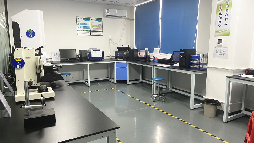
Every production batch undergoes comprehensive electromechanical characterization testing:
As the semiconductor industry advances toward 2.5D/3D packaging structures and heterogeneous chiplet integration, the engineering requirements for wafer test probes are changing rapidly. The technology roadmap focuses on three main developments:
Developing probe diameters smaller than 50 microns to support tight micro-bump pitches (below 80um). This is critical for next-generation system-on-chip (SoC) architectures fabricated on advanced nodes.
Testing automotive and industrial chips requires stable operation under extreme thermal conditions, ranging from -55°C up to +175°C. Selecting materials with low thermal expansion (CTE mismatch mitigation) is essential.
Optimizing probe shapes to minimize parasitic inductance and capacitance, allowing distortion-free signal transmission at testing frequencies exceeding 50 GHz for 5G/6G RF and high-speed data transceivers.
Rongqiangbin's R&D efforts focus on optimizing spring contact internal geometry, plunger profiles, and raw material alloys. Our goal is to provide custom ODM solutions that meet these high-frequency, high-reliability needs while maintaining competitive manufacturing costs.
Addressing the technical, material, and logistical concerns of procurement managers and test engineers.
Explore our specialized range of customized spring-loaded connector pins, sockets, and magnetic interconnect components.
 Rongqiangbin