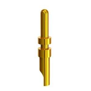
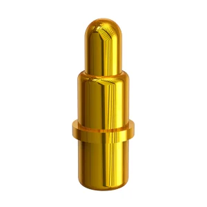
Explore our flagship industrial spring-loaded contacts and custom interfaces deployed globally for semiconductor testing and reliability verification.
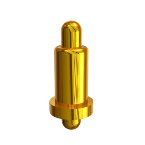
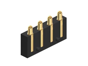
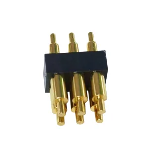
An industry whitepaper examining high-frequency, high-reliability test sockets in global chip validation paradigms.
In the rapidly advancing landscape of semiconductor packaging and device verification, custom testing sockets serve as the indispensable physical bridge between the Integrated Circuit (IC) device under test (DUT) and the Automated Test Equipment (ATE). As chip architectures shrink toward sub-3nm nodes and transition to Heterogeneous Integration (HI) or Chiplet configurations, standardized socket configurations often fail to meet the tight tolerance requirements of high-speed RF, wafer-level, and complex system-on-chip (SoC) verification pipelines.
Custom testing sockets are highly engineered, mechanical-electrical fixtures designed to match the precise footprint, pitch, and pin layouts of diverse chip package architectures, including BGA (Ball Grid Array), LGA (Land Grid Array), QFN (Quad Flat No-Leads), and WLCSP (Wafer Level Chip Scale Packaging). These sockets must operate flawlessly across tens of thousands of insertion cycles, maintaining low and stable contact resistance, structural integrity under thermal extremes, and exceptional signal purity at frequencies soaring above 50 GHz.
The global semiconductor test socket market is undergoing a structural expansion driven by the exponential demand for high-performance computing (HPC), artificial intelligence (AI) chipsets, automotive radar modules, and 5G/6G millimeter-wave telecommunications infrastructure. North American, European, and Asian chip designer firms require highly customized, rapid-prototype testing sockets to accelerate their time-to-market. Leading manufacturers in regional hubs like Shenzhen, China—a core zone within the Guangdong-Hong Kong-Macao Greater Bay Area—offer unparalleled advantages in raw material sourcing, ultra-precision CNC tooling, and rapid turnaround cycles, making them strategic partners for multinational chip design houses and ATE integrators.
The evolution of high-performance test interfaces to meet the needs of advanced semiconductor packaging.
Modern RF IC testing requires sockets with insertion losses under -1dB at 40GHz to 80GHz. Custom co-axial probes and specialized dielectric plastics (such as PEEK and Torlon) prevent capacitive coupling and maintain signal path matching.
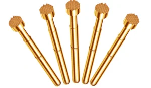
As mobile devices adopt ultra-dense packaging like WLCSP, contact pitch dimensions have scaled down to 0.3mm, 0.2mm, and even smaller. Achieving consistent spring force at this micro-scale requires advanced micro-machined pogo pins built with custom alloy combinations.
Reliability testing protocols (such as Burn-In and HTOL) demand socket housings that can withstand wide temperature sweeps without mechanical deformation. We optimize CTE (Coefficient of Thermal Expansion) mismatch between the semiconductor package and socket body.
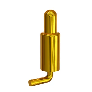
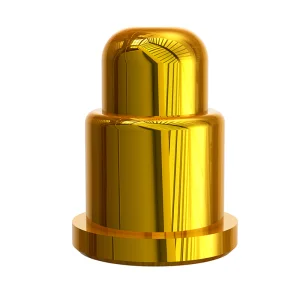
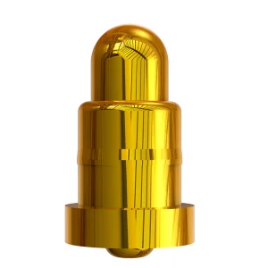
Founded in February 2011 in Songgang Street, Shenzhen, Shenzhen Rongqiangbin Electronic Hardware Co., Ltd. is strategically located in the leading city of the Guangdong-Hong Kong-Macao Greater Bay Area. Over years of development and technical deposition, our company has become a recognized leader in the R&D, manufacturing, and distribution of high-performance POGO PIN connectors (spring thimble assemblies) and custom testing socket contact elements.
We are dedicated to the pursuit of structural perfection. Driven by our philosophy of "excellent quality, intimate service" and core value of "customer-centric, create more value for customers," we have established long-term cooperative partnerships with a vast roster of globally distinguished technology giants.
Our core strengths include high-speed precision lathes, automated assembly lines, a robust environmental management protocol, and a dedicated engineering team capable of rapid customization to meet complex electrical, mechanical, and frequency parameters.

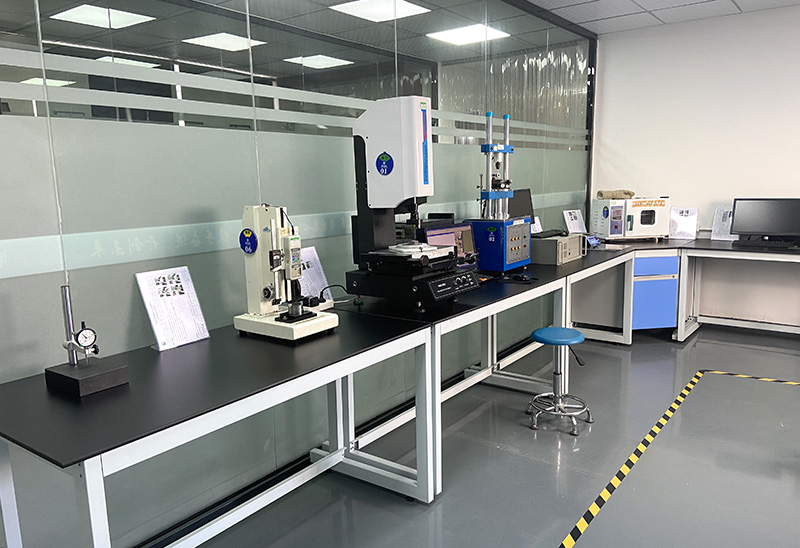
Peek inside our advanced facility equipped to handle complex micro-precision fabrication and stringent quality controls.
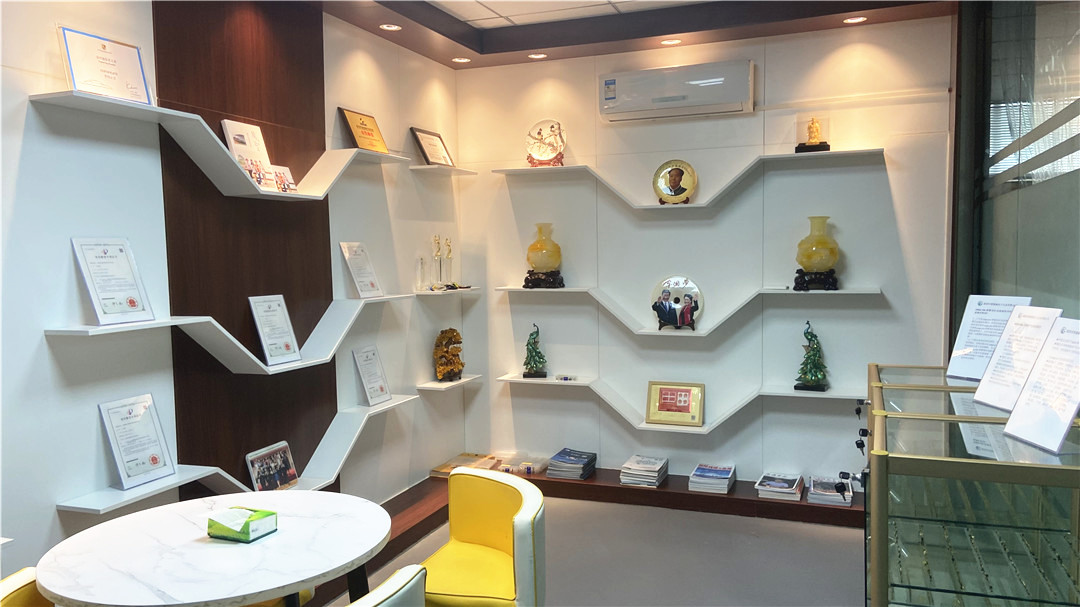
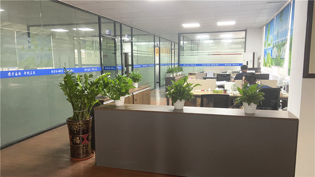
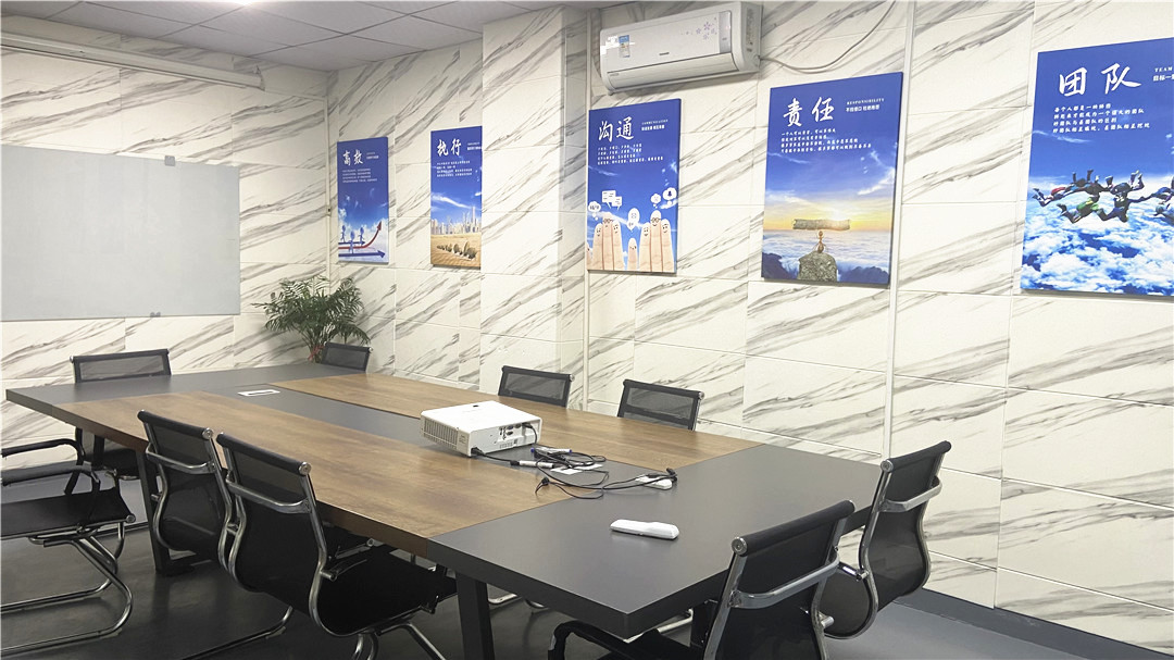
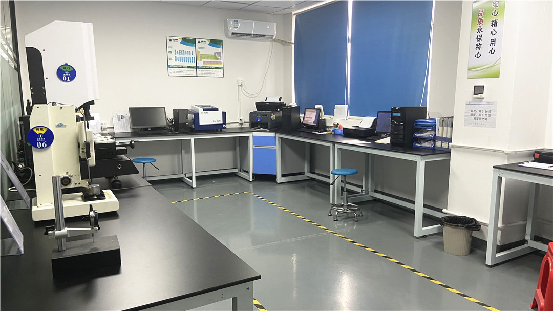
Pioneering standard-setting engineering for prominent companies across multiple high-tech verticals.
Our vision is clear: "Committed to be excellent POGO PIN manufacturers for both quality and cost at home and abroad, and leading connector technology development." Through the relentless refinement of production methods, raw material sourcing, and specialized electroplating, we continuously lower contact resistance and lengthen mechanical lifespans while lowering production cost overheads.
Our corporate spirit centers on the "customer first, integrity first" principle. Supported by a robust quality management team and a comprehensive environmental management system, we provide products that comply with strict RoHS, REACH, and environmental protection declarations. This steadfast reliability has enabled us to secure long-term contracts and strategic partnerships with industry-leading entities, including:
Honeywell, Samsung, SIEMENS AG, ZTE, 360, QCY, HAYLOU, Shanghai Laimu, Luxshare Group, Aoni Electronics, Amphenol Group, and other renowned international enterprises.
We provide specialized connection solutions tailored to high-density interfaces in a broad array of demanding applications:
From raw rod materials to sub-micron finishing, examine our three pillars of manufacturing superiority.
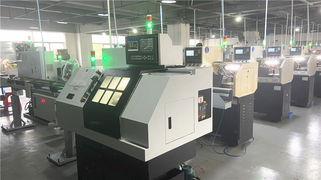
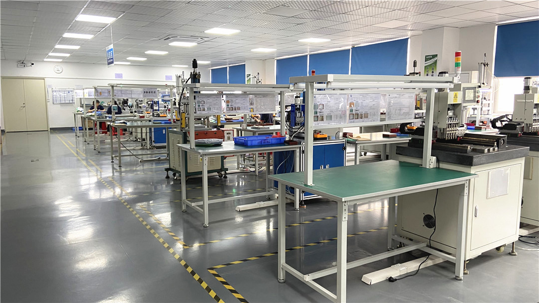
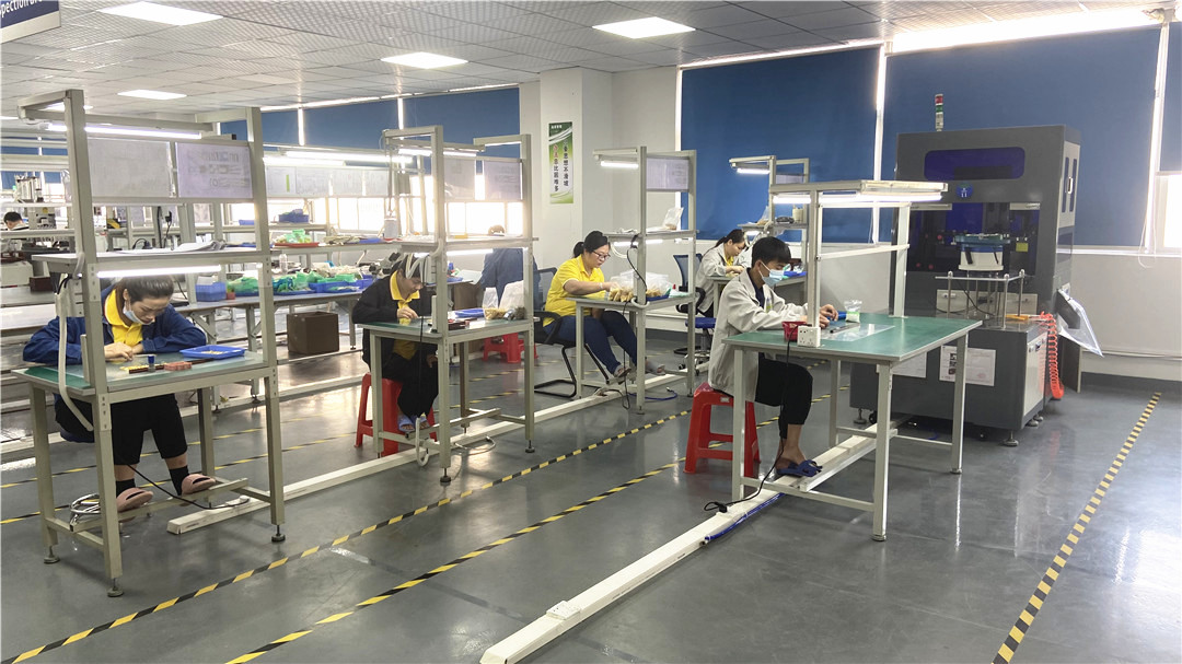
At Rongqiangbin, our production workflow is strictly managed. Our Lathe Section utilizes Swiss-type precision CNC lathe machining center arrays to produce thimbles, plungers, and barrels with tight tolerances of down to ±0.005mm. The Assembly Workshop operates semi-automated and automated insertion tools that integrate internal springs, plungers, and caps without compromising raw material coatings.
Finally, our Inspection & QA Center subjects production batches to dynamic contact resistance testing, spring force displacement calibration, environmental chamber aging (salt spray, humidity, thermal cycle), and high-frequency vector network analysis (VNA) to ensure absolute electrical stability during high-frequency IC test sequences.
Pioneering future-proof technologies to match the evolutionary trajectory of advanced packaging.
Refining 0.25mm pitch pogo pin manufacturing lines for BGA and WLCSP packages. Implementing coaxial shielding directly within micro-socket bodies to maximize signal fidelity up to 40 GHz.
Developing diamond-like carbon (DLC) and advanced palladium-alloy coatings to extend pin lifecycle limits beyond 1,000,000 insertions, reducing maintenance downtime for wafer-level testing.
Integrating micro-sensors directly within socket blocks to monitor real-time mechanical force, temperature, and electrical drift, enabling predictive maintenance in automated smart factories.
Expert technical insights regarding custom testing socket specifications, configuration, and material science.
Selecting the right custom test socket partner requires analyzing three key capabilities: mechanical precision, electrical proficiency, and material compatibility. The manufacturer must offer CNC lathe tolerances of ±0.005mm or better, have experience designing coaxially shielded pins for high frequencies, and provide certified materials like Torlon, PEEK, or Vespel for socket bodies to prevent thermal degradation during high-temperature testing.
Rongqiangbin (RQB) spring pins utilize gold-plated plungers and barrels over high-performance base alloys. Gold plating provides excellent electrical conductivity and prevents oxidation. Furthermore, we optimize the internal spring preload force (typically between 15g to 40g depending on pitch) to reliably break through any oxide layers on the chip solder balls or pads, ensuring a stable contact resistance (under 50mΩ) throughout the testing cycle.
Yes. RQB designs custom socket configurations containing coaxial structures, ground pins, and specialized geometries optimized using electromagnetic field simulation tools. These configurations minimize insertion loss (S21) and return loss (S11), enabling reliable testing of RF power amplifiers, Wi-Fi 6E/7 ICs, and 5G transceiver modules.
Our manufacturing facility has obtained the international authoritative ISO9001:2015 version quality management system certification. We operate under a highly disciplined environmental management framework, checking all outgoing product batches with optical coordinate measuring machines, force displacement testers, and impedance meters to ensure complete conformity to custom customer drawing criteria.
Thanks to our localized manufacturing cluster in Songgang Street, Shenzhen, we can compress the engineering and prototyping cycle. Simple socket designs can be modeled and manufactured within 7 to 10 working days, while highly complex coaxially shielded custom IC test blocks take 2 to 3 weeks, including rigorous validation cycles prior to delivery.
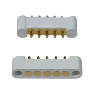
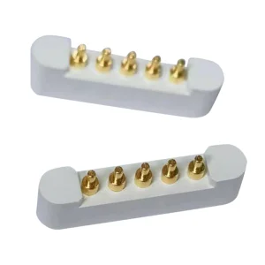
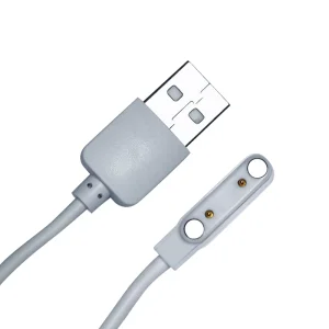
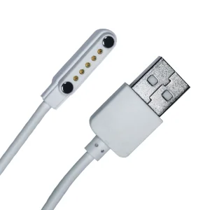
Our second array of specialized connector assemblies, charging interfaces, and heavy-duty current contact sockets.
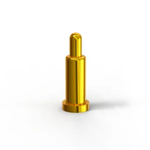
Send us your pitch layouts, device packaging datasheets, and target application requirements. Our engineers will provide custom solutions tailored to your ATE environment.
Contact Our Technical Team Rongqiangbin